


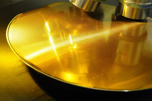
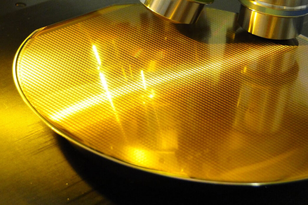
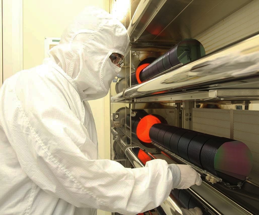
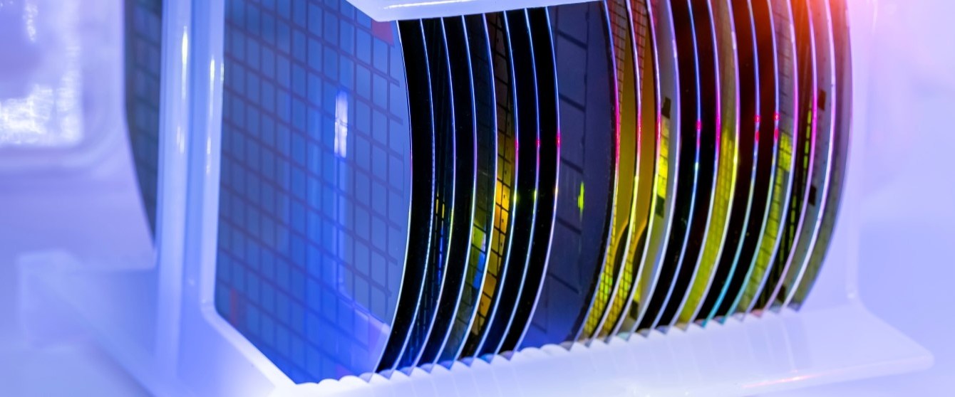
A semiconductor wafer at CEITEC’s Porto Alegre facility. (Source: CEITEC)
Homerun Resources Inc. is moving further up the technology ladder. Its latest step reaches into one of the key materials shaping the future of power electronics: Silicon carbide (SiC) substrates and wafers. Today, the company announced a Memorandum of Understanding with CEITEC S.A., Brazil’s federally owned semiconductor company, creating a bridge between Homerun’s upstream materials strategy and Brazil’s emerging SiC manufacturing ambitions.
According to the news-release, the cooperation is aimed at developing, producing and qualifying SiC substrates and wafers for semiconductor applications, with the goal of helping establish a more complete domestic SiC value chain.
The bigger picture is becoming increasingly clear: Homerun is no longer looking only at the resource in the ground, but at the technological pathway that could ultimately connect its silica to the semiconductor industry.
What makes the announcement especially significant is who Homerun is working with. CEITEC is a state-owned semiconductor company headquartered in Porto Alegre and linked to Brazil’s Ministry of Science, Technology and Innovation. It already operates semiconductor manufacturing infrastructure and has been repositioned as an important part of Brazil’s move into next-generation power electronics.
Brazil is already investing substantial public capital to modernize CEITEC for wide-bandgap semiconductors, with SiC at the center of the strategy. The goal is to strengthen Brazil’s semiconductor industry, reduce dependence on imported technology and keep more of the economic value created by advanced manufacturing inside the country.
For Homerun, this creates an important link further down the semiconductor value chain. The company is entering a Brazilian industry where SiC has already been identified as a priority technology, manufacturing capacity is being expanded and government support is helping build a domestic semiconductor industry with growing technical and industrial depth.
The opportunity is therefore to take Homerun’s high-purity silica sand further down the value chain toward SiC substrates, wafers and ultimately semiconductor applications inside Brazil.
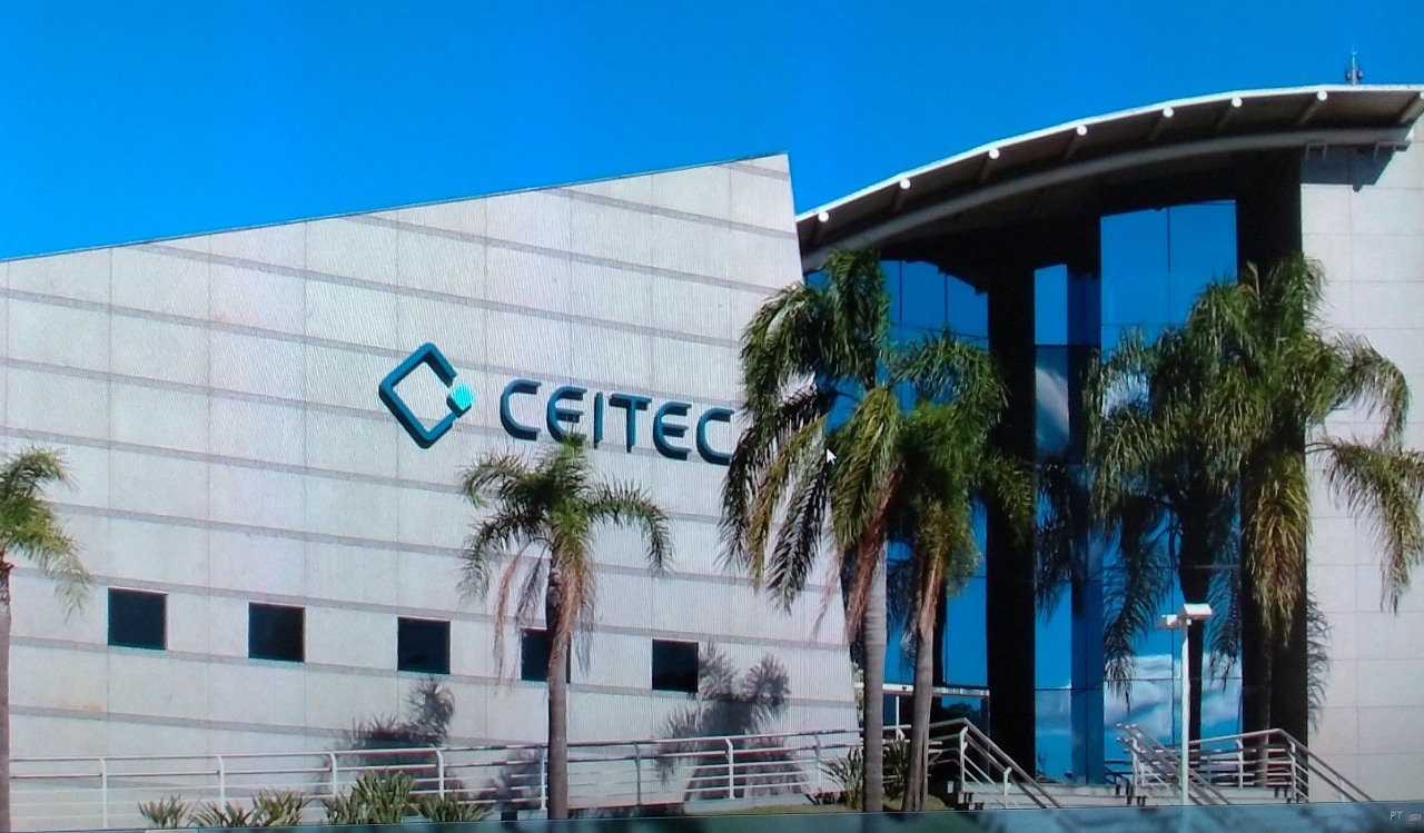
CEITEC: BRAZIL’S STATE-OWNED SEMICONDUCTOR COMPANY
CEITEC, short for Centro Nacional de Tecnologia Eletrônica Avançada, was established in 2008 by presidential decree as a federal public company to help develop Brazil’s semiconductor and microelectronics industry.
Over the years, the company has developed and manufactured integrated circuits for applications including RFID, identification, authentication, logistics and asset tracking. That operating history gives CEITEC practical manufacturing experience beyond purely academic or laboratory research.
SEMI, a semiconductor industry association, lists CEITEC as a semiconductor device manufacturer and describes the company as part of Brazil’s efforts to develop domestic microelectronics capabilities.
CEITEC’s recent history also shows how semiconductor manufacturing has moved higher on Brazil’s political agenda. A privatization and corporate dissolution process initiated in 2021 was later suspended and ultimately reversed, restoring CEITEC to its role as a strategic public company. Its new direction is particularly relevant to Homerun because Brazil is now repositioning CEITEC toward a more advanced field: Power devices based on wide-bandgap materials such as silicon carbide.
CEITEC’s 2024 management report describes a government-backed project intended to introduce SiC power-device manufacturing technology into Brazil. The program aims to strengthen semiconductor manufacturing and R&D while moving CEITEC into a technology increasingly used in electrification, energy efficiency and decarbonization.
BRAZIL IS PUTTING REAL MONEY BEHIND SILICON CARBIDE
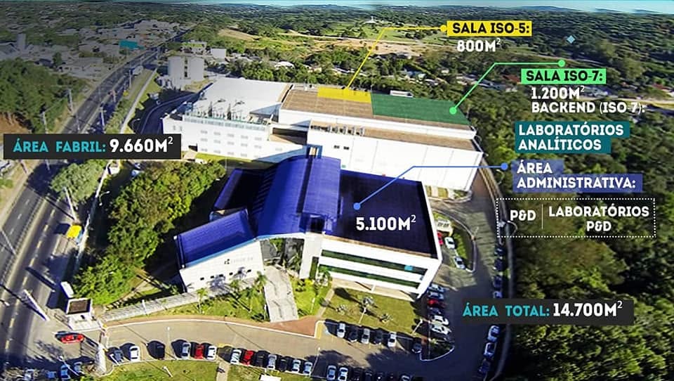
The scale of Brazil’s commitment provides important context for Homerun. CEITEC’s SiC program has a total value of 220.36 million BRL (currently 43 million USD), with funding intended for the adaptation and modernization of its industrial platform.
According to CEITEC, the capital is being directed toward repairing and upgrading production equipment, purchasing new machinery, modifying cleanroom layouts, acquiring technology and implementing the manufacturing processes required for the new SiC route. This gives the program a clear industrial focus, with funding aimed at physical production infrastructure as well as technical capability.
The investment shows that CEITEC’s move into SiC is part of a broader industrial program, not simply a research project. Brazil wants to build capabilities still concentrated among relatively few countries and companies and keep more of the semiconductor value chain at home. That includes materials, processing expertise and manufacturing infrastructure needed to support a domestic ecosystem.
Against this backdrop, Homerun’s cooperation with CEITEC becomes more significant. Today’s news envisages CEITEC contributing semiconductor requirements, manufacturing expertise and validation capabilities, while Homerun intends to work on high-purity SiC materials, substrates, wafers and the processing steps required to move those materials toward semiconductor specifications. This connection could become important if Homerun succeeds in moving beyond high-purity raw-material supply. Semiconductor materials must ultimately meet the specifications of the devices built on them. Working with a downstream manufacturer can therefore give Homerun clearer targets for what its materials need to achieve.
SiC: BUILT FOR HIGHER POWER
Almost every modern electrified system depends on power electronics. These semiconductors switch, convert and control electricity, allowing power to move efficiently between batteries, motors, electrical grids, renewable-energy systems and electronic equipment. Their role becomes more important as vehicles, industry and energy systems move toward higher power levels. As power densities rise, efficiency, heat management and demanding electrical conditions become more important.
SiC is attractive because it is a wide-bandgap semiconductor, allowing it to handle conditions that conventional silicon finds more difficult. Compared with conventional silicon power devices, SiC devices and modules can operate at higher voltages, temperatures and switching frequencies while reducing losses and enabling more compact systems. This can reduce cooling requirements, increase power density and improve conversion efficiency. These properties have made SiC increasingly important in electric vehicles, charging infrastructure, renewable-energy inverters, energy storage, industrial systems and high-performance power supplies.
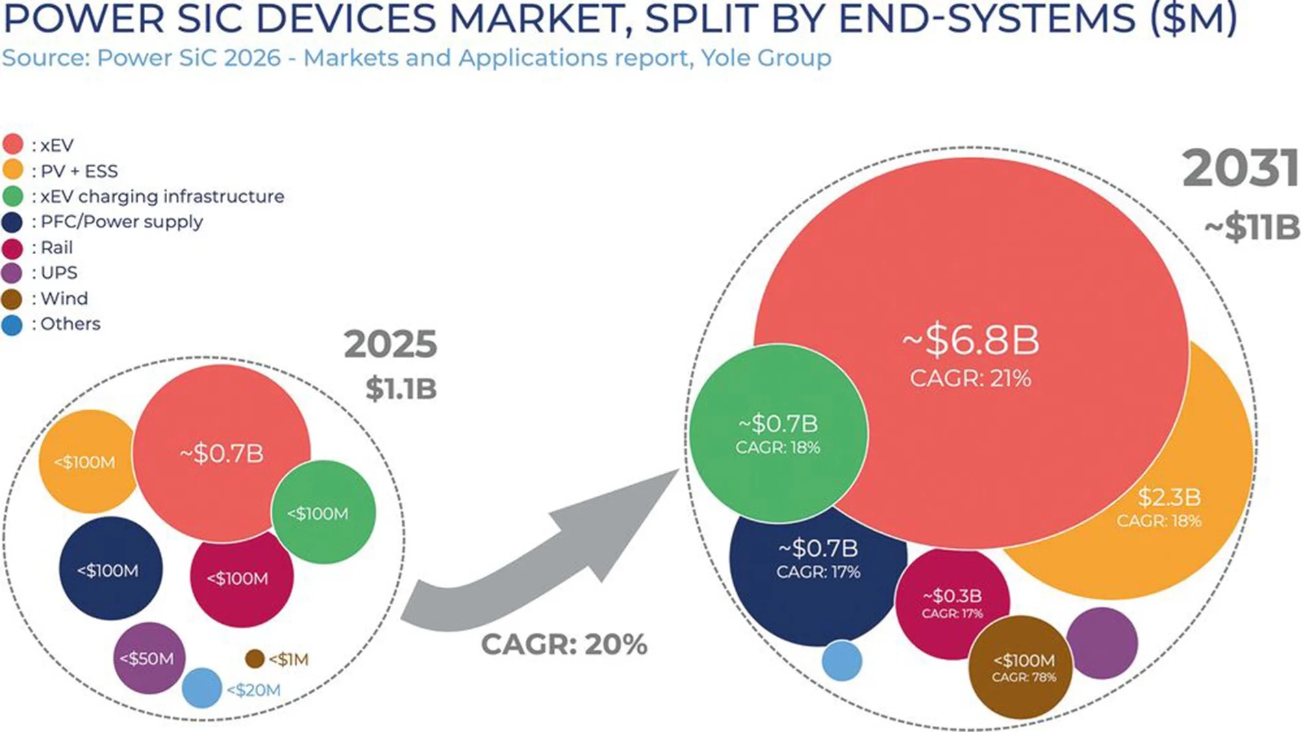
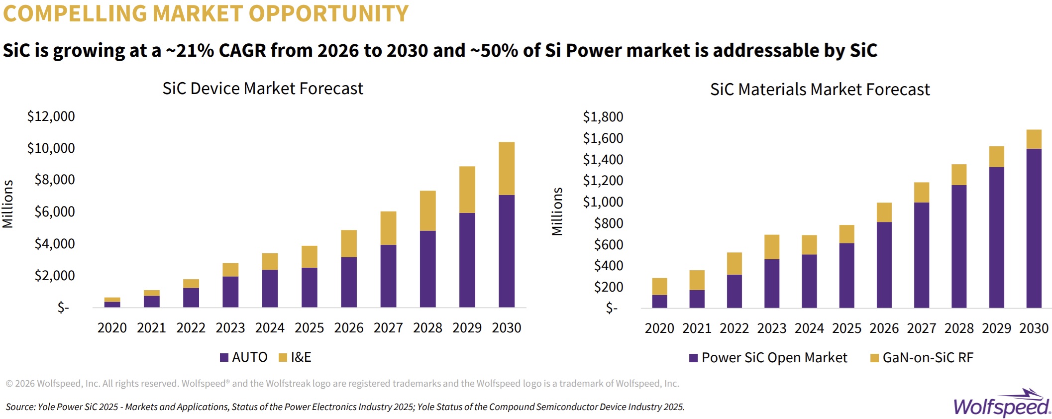
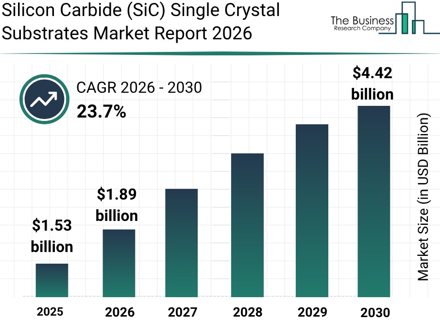
The commercial market is already substantial and continues to expand rapidly. Yole Group forecasts the global power SiC market to reach 11 billion USD by 2031, representing a compound annual growth rate of about 20% between 2025 and 2031. The research firm sees the next growth phase being driven by a broader combination of 800 V electric vehicles, renewable energy, industrial applications, data centers and continuing investment in 200 mm SiC manufacturing.
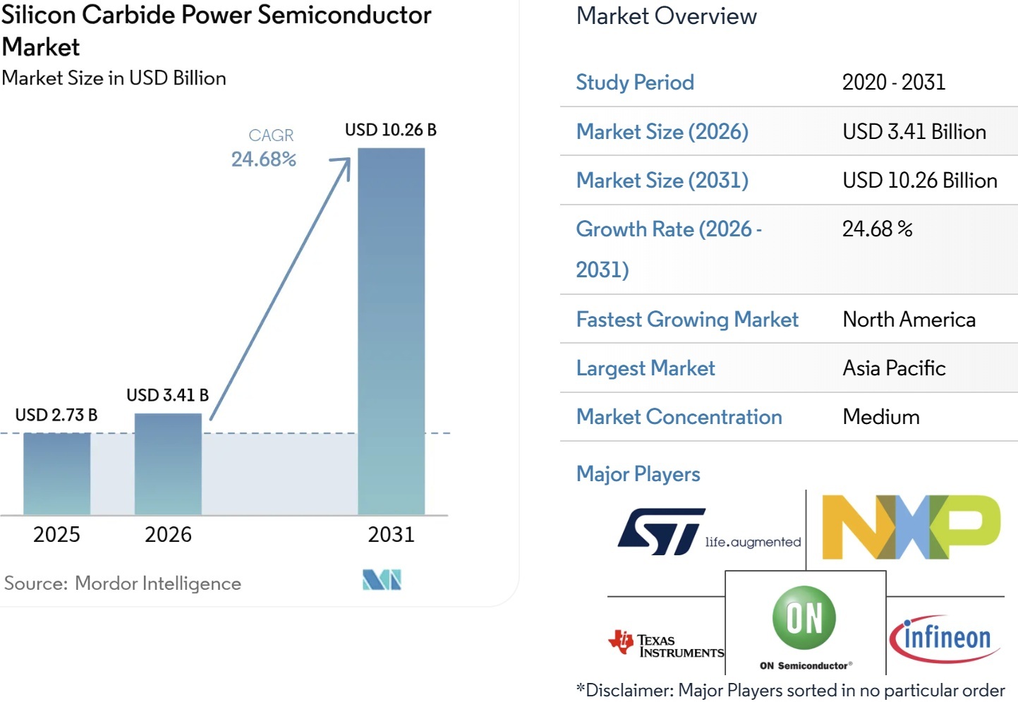
A separate 2026 market assessment by Mordor Intelligence estimates the SiC power-semiconductor market at 3.41 billion USD in 2026 and projects it to reach 10.26 billion USD by 2031, equivalent to a CAGR of almost 25%. Forecasts vary depending on how the market is defined, but the direction is clear: SiC is becoming increasingly important in high-power electronics.
BEYOND ELECTRIC VEHICLES
Electric vehicles remain the largest commercial market for SiC today. Mordor Intelligence estimates that automotive applications accounted for 61% of global SiC power-semiconductor revenue in 2025, reflecting adoption in traction inverters, onboard chargers, DC-DC converters and charging infrastructure. The same research anticipates fast-charging infrastructure to be one of the industry’s fastest-growing application areas through 2031. That concentration is beginning to ease as SiC adoption spreads into other high-power markets.
At the same time, the market is becoming more diversified. Renewable-energy installations require increasingly efficient conversion electronics, battery-storage systems need high-power bidirectional converters and industrial facilities are electrifying processes that previously relied on mechanical or fossil-fuel-based systems. AI data centers are emerging as another major source of demand as their enormous electrical loads force operators to rethink how power is distributed and converted inside increasingly dense computing facilities. This broadening demand base could become increasingly important for future SiC growth.
This diversification matters because it reduces the industry’s dependence on the automotive cycle that drove much of the original SiC investment boom. Yole’s latest outlook specifically highlights renewables, industrial applications and AI data centers alongside electric vehicles as contributors to the next phase of market growth.
ELECTRIC VEHICLES AND ULTRA-FAST CHARGING
The automotive industry has been one of the principal forces behind commercial SiC adoption. The shift toward 800 V vehicle architectures makes efficient power conversion increasingly important because higher voltages enable faster charging and can reduce losses across the drivetrain. This can improve vehicle efficiency while also supporting shorter charging times at high-power stations. SiC has consequently become an increasingly important material for traction inverters, onboard chargers and high-power charging equipment.
The industry continues moving toward even higher-voltage platforms. Recent market research notes that EV manufacturers are increasingly standardizing around 800 V systems, where SiC offers particularly attractive performance characteristics. The market already reflects this shift: According to Mordor Intelligence, the 600-900 V segment accounted for more than half of SiC power-semiconductor revenue in 2025.
CEITEC has itself identified electric-vehicle control systems as one of the intended application areas for its SiC manufacturing program. That creates a potential Brazilian link between advanced SiC materials and one of the fastest-growing areas of transportation technology.
SOLAR POWER, ENERGY STORAGE AND THE MODERN GRID
For Homerun, the renewable energy connection is particularly relevant because it links the SiC strategy back to the company’s existing solar business. A photovoltaic module produces direct current, but that electricity must be converted before it can be used by most consumers or fed into the grid. Power semiconductors inside solar inverters perform this function, while battery storage systems require high-efficiency power conversion during both charging and discharging.
SiC can improve the efficiency and power density of these systems, especially at high voltages. This makes it increasingly attractive in utility-scale solar, storage and grid applications where even small improvements in conversion efficiency can translate into meaningful energy savings across large installations.
CEITEC has explicitly highlighted solar energy conversion systems among the applications for its planned SiC power devices. For Homerun, that creates an interesting connection across its broader strategy: The company’s high-purity silica could potentially serve the energy transition through both solar glass and advanced materials used in the power electronics that manage the electricity generated by those same systems.
That connection becomes more important as solar and energy-storage installations continue to grow worldwide. SiC increasingly occupies the high-voltage portion of the power-semiconductor market, where conventional silicon becomes less efficient and where the performance advantages of wide-bandgap materials become more pronounced.
AI DATA CENTERS ADD A NEW SiC GROWTH DRIVER
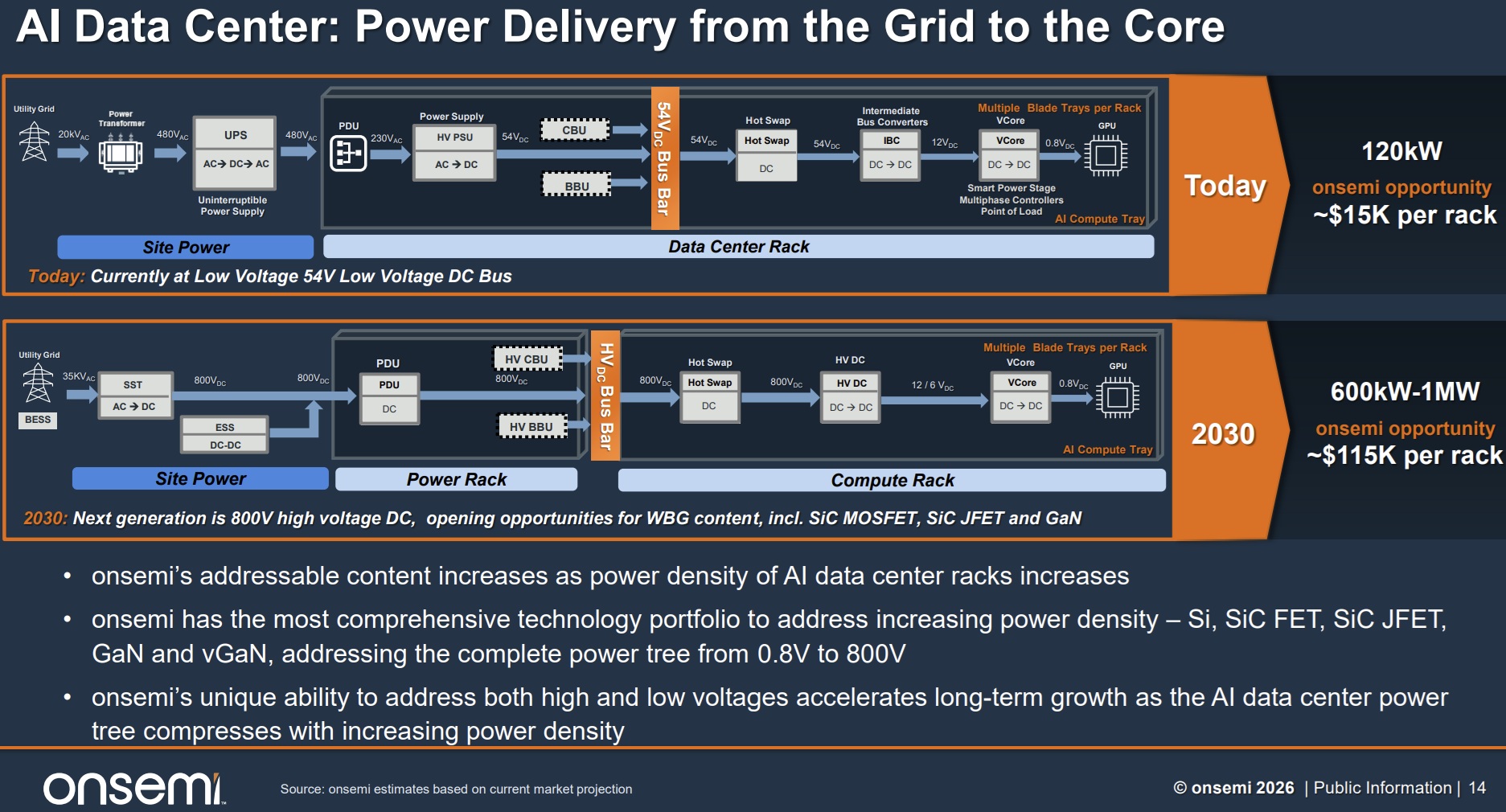
The AI infrastructure boom is creating a new growth market for power semiconductors. AI is usually discussed in terms of GPUs, memory and optical connectivity, but the power infrastructure needed to run these systems is becoming an equally important challenge.
Large AI data centers consume enormous amounts of electricity, and that power must pass through several conversion and distribution stages before reaching the processors. As computing density rises, power losses generate increasing amounts of heat and place additional pressure on cooling systems. Improving efficiency across the power chain therefore becomes increasingly valuable as next-generation AI racks move toward much higher power densities.
- Recent industry announcements show how quickly SiC is moving into AI infrastructure: In August 2026, Wolfspeed and LITEON announced a partnership targeting next-generation hyperscale AI data centers using 800 VDC power architectures. Wolfspeed’s SiC technology has been qualified for LITEON’s 800 VDC sidecar power platform and compute-rack power supply systems, with the companies specifically pointing to the scalability of Wolfspeed’s 200 mm SiC manufacturing platform.
- Wolfspeed’s own financial results provide another useful indication of the trend: The company reported that its AI data-center revenue more than doubled year-over-year during fiscal 2026 and described data centers as its fastest growing end market, albeit from a comparatively smaller base within its overall business mix.
- Infineon and Siemens also announced a collaboration in June 2026 using SiC power modules in semiconductor circuit breakers designed for data centers, factories and battery storage systems. The objective is to improve power density, efficiency and reliability in electrical protection systems.
- The trend has continued: On September 9, 2026, Infineon and SolarEdge announced an expansion of their cooperation around solid-state circuit breakers for 800 VDC AI data-center power architectures, aimed at enabling faster electrical protection and more efficient end-to-end DC power distribution from the grid connection toward computing racks.
These developments illustrate how SiC is moving into another major infrastructure market. The AI buildout requires more than computing chips; it increasingly depends on technologies capable of delivering enormous amounts of electricity efficiently, reliably and at very high power densities.
THE ROAD TO HIGH-PURITY SEMICONDUCTOR-GRADE SiC
SiC is not a new material. Industrial SiC has been used for more than a century in abrasives, ceramics, refractories and other high-temperature applications. Semiconductor-grade SiC, however, is far more demanding. Purity, crystal quality, defects and consistency become critical because even small imperfections can affect device performance.
Producing a semiconductor wafer requires far more than making SiC powder. Single crystals must be grown under tightly controlled conditions, sliced into wafers and polished to demanding specifications before semiconductor devices can be built on them.
The simplified material chain is:
High-purity silica –> silicon –> high-purity SiC material –> single-crystal growth –> SiC boule –> wafer slicing and polishing –> epitaxy –> semiconductor device
Each step requires greater technical know-how, tighter process control and additional capital. The material’s potential value can also rise sharply as fewer producers are able to meet semiconductor-grade specifications.
This is where Homerun’s advanced-materials strategy becomes particularly interesting. Its opportunity may depend less on the quantity of silica it can produce and more on how far that material can be upgraded before it leaves Brazil.
Silica is the starting point. Purification is followed by silicon and increasingly advanced SiC materials, while single crystals and qualified wafers sit further downstream, where technical performance increasingly determines economic value.
THE STRATEGIC ROLE OF SiC SUBSTRATES AND WAFERS
The SiC substrate is the physical foundation on which the semiconductor device is built. Defects inside the crystal can affect device performance and manufacturing yield, making crystal growth and wafer preparation crucial parts of the entire semiconductor process.
This gives the substrate an importance that goes well beyond its physical size: It can influence how many usable devices ultimately emerge from a wafer and how reliably those devices perform. This is one reason the SiC industry has historically been more vertically integrated than conventional silicon. Major producers have sought greater control over crystal growth, substrate production, epitaxy and device fabrication because limitations at the materials stage can constrain the performance and economics of the finished semiconductor.
The Homerun-CEITEC cooperation is therefore targeting a technically important part of the value chain. According to the news-release, Homerun intends to develop and coordinate raw material processing and manufacturing steps associated with semiconductor-grade SiC substrates and wafers, while CEITEC is expected to contribute specifications, semiconductor manufacturing expertise and technical validation.
For a materials developer like Homerun, understanding what a semiconductor manufacturer actually needs can be extremely valuable. It allows development work to focus on specifications that matter commercially and can ultimately support customer qualification, rather than pursuing purity or processing targets in isolation. That direct feedback loop can help align research and process development with real-world manufacturing requirements from the beginning.

THE GLOBAL RACE TOWARD 200 MM SiC
One of the clearest signs of the industry’s development is the shift from 150 mm, or 6-inch, wafers toward larger 200 mm, or 8-inch, wafers. Larger wafers allow more chips to be produced from each substrate and can lower manufacturing costs as yields improve.
For manufacturers, the attraction is straightforward: More usable chip area can be processed during each manufacturing cycle, spreading fixed processing costs across a larger number of devices.
The scale of investment is considerable:
- STMicroelectronics is developing an integrated SiC campus in Catania, Italy, that brings together substrate development, epitaxy, 200 mm front-end wafer manufacturing, packaging and R&D. The company expects the facility to ramp toward capacity of up to 15,000 wafers per week at full build-out.
- Wolfspeed’s latest generation of SiC MOSFETs is meanwhile being produced on the company’s qualified 200 mm manufacturing platform. The company says the larger platform provides customers with a scalable route toward next-generation automotive and industrial SiC products, while supporting higher-volume production and improved manufacturing economics over time.
The shift to 200 mm is still at an early stage. Mordor Intelligence estimates that 150 mm substrates accounted for more than 72% of the SiC power-semiconductor market in 2025, while 200 mm wafers represent one of the industry’s important growth areas. For new entrants, the technical bar is therefore getting higher. Crystal quality must improve, defects must decline, wafer diameters are increasing and manufacturing costs are falling as established producers scale.
That evolution raises the importance of getting the underlying materials and processing technologies right before large-scale manufacturing begins.
GOVERNMENTS ARE TREATING SiC
AS STRATEGIC TECHNOLOGY
Brazil’s support for CEITEC fits into a broader international trend. Governments increasingly view wide-bandgap semiconductors as strategic technologies because they are becoming important in energy infrastructure, transportation, advanced manufacturing and defense. As countries compete to secure critical technology supply chains, domestic access to advanced power semiconductors is becoming increasingly important for industrial resilience and technological independence.
- In June 2026, the U.S. Department of Commerce awarded 250 million USD under the CHIPS R&D program to I-Pulse to develop next-generation SiC semiconductors capable of operating under extreme high-temperature, high-current and high-voltage conditions. The program involves cooperation with federal laboratories, universities and specialist manufacturers.
- Only a few weeks later, the U.S. Department of Commerce announced another major SiC investment: Up to 225 million USD in CHIPS incentives for Bosch, supporting a planned 2 billion USD transformation of the company’s Roseville, California facility into a state-of-the-art SiC semiconductor plant. Bosch expects the site to become its largest SiC manufacturing facility globally.
- The trend is extending into increasingly advanced applications as well: In June 2026, GE Aerospace and Wolfspeed announced cooperation around high-voltage SiC solutions, including 10 kV MOSFETs, with potential applications in industrial electrification, aerospace, defense and power infrastructure associated with AI. This broadening application base is one reason governments are treating SiC as more than just another semiconductor technology.
These investments show how strategically important SiC has become. SiC is becoming part of national industrial strategies because efficient power electronics increasingly sit at the center of electrification, renewable-energy integration, AI infrastructure and advanced manufacturing.
The competition is therefore increasingly about more than simply producing devices. It also involves securing the materials, manufacturing know-how, infrastructure and qualified supply chains needed to support those devices at scale.
BRAZIL MOVES UP THE SEMICONDUCTOR VALUE CHAIN
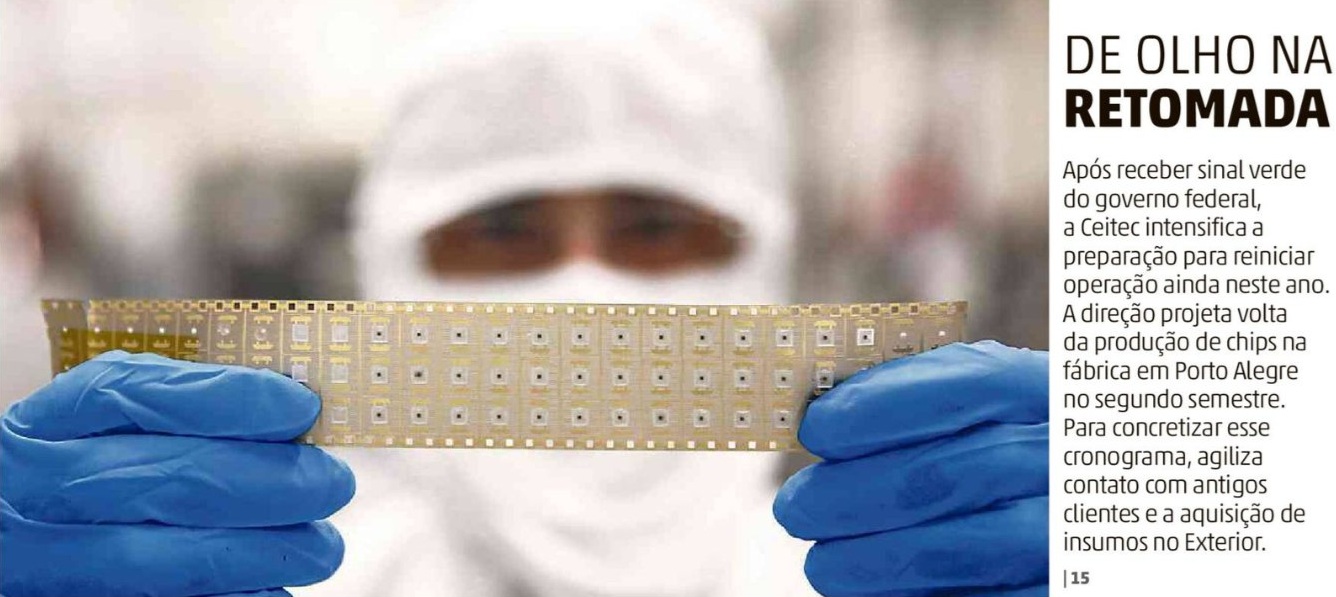
CEITEC’s transformation is part of Brazil’s broader push to build semiconductor manufacturing, research and technology domestically. The logic is straightforward: Semiconductors are essential to vehicles, telecommunications, renewable energy, industrial automation, defense, medical equipment and digital infrastructure. Dependence on foreign suppliers therefore creates economic and strategic risks.
Brazil’s current position shows why this has become such an important industrial objective:
- According to ABINEE’s 2026 industry overview, the country imported 5.96 billion USD of semiconductors in 2025, following 6.31 billion USD in 2024, making semiconductors one of Brazil’s largest categories of imported electrical and electronic products.
- At the same time, Finep estimates that Brazil’s domestic semiconductor industry will generate around 2.5 billion USD in revenue in 2026.
- In other words, the scale of semiconductor imports remains significantly larger than the revenues generated by the domestic industry, highlighting the country’s continued dependence on foreign supply.
Brazil wants to do more than simply produce more chips: It wants to capture a larger share of the entire semiconductor value chain. Finep has stated that the country aims to increase its participation from roughly 1% today to around 2% by 2033, effectively doubling its position in the global industry. Reaching that goal will require more than chip factories. Brazil also needs capabilities in materials, processing, equipment, chip design, packaging, research and qualification. That broader ecosystem is essential if Brazil wants to retain more technological know-how and economic value domestically. Building those capabilities around domestic raw materials could create an additional advantage by connecting resource security with increasingly sophisticated manufacturing expertise.
This is where Homerun’s strategy could fit into the bigger picture. Brazil possesses abundant mineral resources and renewable energy, yet a large share of the value associated with transforming those inputs into advanced technology products has historically been created elsewhere. A high-purity silica resource in Bahia becomes much more interesting if the material can be processed inside Brazil into purified silica, silicon, SiC, substrates and wafers instead of leaving the country mainly as raw material.
For Homerun, the opportunity therefore aligns closely with Brazil’s wider industrial ambition. The more domestic value that can be added between the mine and the finished technology product, the more strategically important the underlying resource can become. That could allow more of the value created from the material to remain in Brazil. In that sense, the company’s effort to move from silica toward increasingly sophisticated semiconductor materials is consistent with the broader national objective of strengthening Brazil’s position higher up the technology value chain.
TURNING SILICA INTO TECHNOLOGY
Homerun’s story begins with an unusually strong raw material foundation. Its silica resources in Bahia combine exceptional purity, very low iron content and consistent chemistry – qualities that become increasingly important as silica is transformed into more advanced technology products. In semiconductor-grade SiC, impurity control, crystal quality and consistency are critical, which means the quality of the starting feedstock has a direct impact on everything that follows, from purification and crystal growth to wafer quality and final device performance.
This is important because the final quality of semiconductor-grade SiC is influenced long before a wafer is produced. Control over impurities begins with the feedstock itself, making the quality and consistency of the original silica increasingly important as processing advances downstream.
That is where Homerun sees a competitive advantage. Only a limited number of silica deposits worldwide offer the combination of purity and consistency required for advanced downstream processing. Homerun’s silica sand belongs to that select group, giving the company a rare starting point as it moves further into the silicon and SiC value chain.
Solar glass was the first major industrial opportunity to emerge from that resource and remains a central part of Homerun’s development strategy. But the same characteristics that make the silica attractive for high-performance glass are now opening the door to a much broader advanced materials story.
The company’s work with the University of California, Davis on advanced purification subsequently expanded the discussion toward much higher-purity materials. The technological pathway now being investigated reaches further into fused silica, silicon, SiC and potentially semiconductor substrates and wafers. Each additional processing step could open access to increasingly specialized and higher-value technology markets.
These markets differ significantly from conventional industrial minerals. They depend on processing technology, intellectual property, material characterization, qualification and manufacturing consistency. As the material moves downstream, tonnes matter less and crystal quality, defects, wafer specifications and device performance matter more.
The CEITEC cooperation adds an important semiconductor connection to this progression. Homerun now has the opportunity to work with a Brazilian semiconductor manufacturer that is itself being equipped for SiC power-device production, providing a potential interface between the company’s upstream materials strategy and the requirements of an actual semiconductor fabrication environment. Working with CEITEC gives Homerun clearer technical targets for the materials it needs to develop. That could be particularly valuable in a field where small differences in purity, crystal quality and consistency can determine whether a material is commercially usable.
A STRATEGIC STEP TOWARD INDUSTRIALIZATION
The 3-year MOU represents the starting point for the cooperation. According to the news-release, the companies intend to identify joint projects, define technical requirements, investigate manufacturing capabilities, involve additional technology partners where required and develop a roadmap toward potential qualification, scaling and industrialization.
The companies intend to translate the broader MOU into structured Work Plans under separate cooperation agreements, potentially turning the framework into defined technical programs with measurable development milestones.
The companies also intend to identify additional technology partners and pursue domestic and international funding for specific technical projects. This approach could allow individual parts of the SiC development chain to be advanced with specialized expertise rather than requiring Homerun to build every capability internally from the outset.
Importantly, the MOU explicitly contemplates Homerun producing semiconductor-grade SiC substrates and wafers for offtake by CEITEC. This creates a direct potential commercial pathway: If Homerun successfully develops and qualifies wafers to CEITEC’s specifications, the MOU expressly contemplates CEITEC as the downstream offtake partner for those products.
Brian Leeners, CEO of Homerun, highlighted how the cooperation could connect the company’s raw material advantage with downstream semiconductor manufacturing in Brazil:
“Partnering with CEITEC, a key semiconductor manufacturer in Brazil, allows us to close the loop on a local, vertically integrated supply chain. By aligning our high-purity feedstocks and rapid processing technologies with CEITEC’s manufacturing and validation expertise, we are positioning Brazil as a powerhouse for advanced Silicon Carbide substrate technologies during a time of intense global supply chain competition. This collaboration is designed to translate raw earth advantages directly into high-barrier deep-tech semiconductor solutions.”
Homerun CEO Brian Leeners in today's news-release
His comments underline the broader logic of the partnership: Homerun is connecting a rare high-purity feedstock with advanced processing, qualification and an established downstream semiconductor manufacturer within the same country. This creates the possibility of building a more complete domestic development pathway in which raw material, processing expertise, wafer development, technical validation and potential future commercial demand are linked much more closely than in a conventional commodity supply model, allowing more technological know-how, industrial capability and economic value to remain in Brazil.
CEITEC is framing the cooperation in similarly strategic terms. Edelweis Ritt, CMO of CEITEC, emphasized both the company’s move toward SiC power devices and the importance of building more of the value chain domestically:
“CEITEC, as Brazil’s strategic state-owned semiconductor company, is advancing its technological repositioning toward SiC power devices. This collaboration with Homerun, leveraging its work on high-purity silica in Brazil, represents an important step toward developing a vertically integrated SiC value chain in the country and strengthening Brazil’s technological and industrial capabilities in a sector that is strategic for the energy transition.”
CEITEC CMO Edelweis Ritt in today's news-release
Her comments are important because they show that the vertical-integration thesis is not being articulated by Homerun alone. CEITEC itself is explicitly linking Homerun’s high-purity silica work with Brazil’s ambition to build a more complete domestic SiC ecosystem. Advancing toward commercial semiconductor-grade substrates opens the next stage of technical development for Homerun. The required processing steps (including advanced thermal processing, single-crystal growth and precision wafer finishing) can be developed internally or together with specialized technology partners.
The value of the cooperation is that Homerun can define those technical requirements together with an actual semiconductor manufacturer. CEITEC is also expected to support physical device validation using qualified substrates and wafers, providing direct engineering feedback that could feed back into Homerun’s material and processing development. That creates the possibility of an iterative development process in which wafer performance is tested, feedback is returned and the material or processing route is refined accordingly.
If the relationship develops into specific projects, each stage could progressively test whether Homerun’s raw material advantage can be translated into competitive advanced semiconductor materials.
GLOBAL SEMICONDUCTOR MARKET MOMENTUM
The Homerun-CEITEC cooperation is taking shape against an exceptionally strong semiconductor market backdrop.
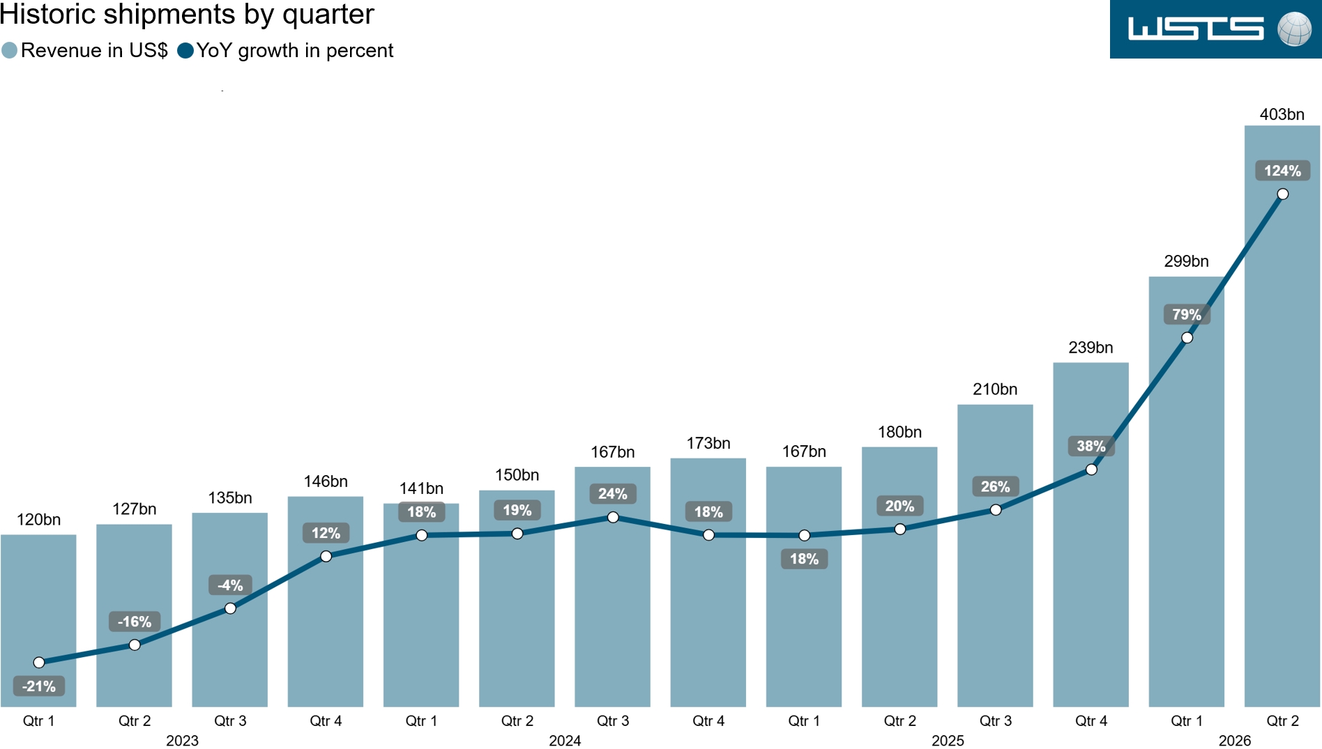
- Global chip sales reached 403.3 billion USD in the second quarter of 2026, up 35.1% from the first quarter, according to the Semiconductor Industry Association.
- By July, monthly global sales had climbed to 146.8 billion USD, more than doubling from a year earlier.
- The World Semiconductor Trade Statistics (WSTS) now calculates that the global semiconductor market could reach 1.65 trillion USD in 2026, driven by AI infrastructure, advanced computing, memory and broader semiconductor demand.
For Homerun, the significance is not simply the size of the chip market, but the growing strategic importance of the materials and manufacturing capacity behind it. As power electronics move toward higher voltages, temperatures and power densities, SiC is becoming increasingly important because its wider bandgap and superior thermal properties allow it to perform where conventional silicon becomes less efficient.
The performance of SiC devices depends heavily on what happens much earlier in the manufacturing chain. Semiconductor-grade SiC requires exceptional purity, tightly controlled crystal growth and very low defect levels, making the quality and consistency of the starting material increasingly important.
This creates a potential advantage for Homerun: Its high-purity, low-iron silica resources in Bahia provide an unusually strong feedstock from which increasingly advanced silicon and SiC materials can be developed. As countries seek more secure and geographically diversified semiconductor supply chains, control over high-purity feedstocks, advanced processing capability, crystal growth, wafer preparation and domestic manufacturing infrastructure is becoming increasingly valuable.
Homerun’s strategy is therefore aimed at addressing the value chain much earlier than the finished semiconductor device, while CEITEC provides the downstream manufacturing and validation connection. Together, the relationship links a rare Brazilian raw material with advanced processing and semiconductor manufacturing within the same country.
If successfully developed, that combination could give Brazil greater control over several stages of a technology chain that is currently concentrated among a relatively small number of global producers.
CEITEC ADDS A CRITICAL DOWNSTREAM INDUSTRIAL LINK
Several pieces of the Homerun story are beginning to fall into place. The company has a high-purity silica resource in Brazil, is developing advanced purification technologies, is investigating increasingly sophisticated silica-derived products and now has a cooperation framework with a state-owned semiconductor company focused on SiC. These elements are beginning to connect rather than developing as isolated initiatives.
At the same time, Brazil is investing more than 220 million BRL in CEITEC’s SiC transformation, while governments and major semiconductor companies elsewhere are committing billions of dollars to the same technological shift.
The global power-SiC market is forecast to grow to 10 billion USD by the beginning of the next decade, with electric vehicles increasingly joined by renewable energy, storage, industrial applications and AI infrastructure as major sources of demand.
The technological challenges remain substantial, particularly in semiconductor-grade purity, crystal growth, wafer quality, defect reduction and customer qualification. Yet those barriers also explain why successful progression through the value chain could have considerably greater economic significance than conventional silica production.
The key question is how far Homerun can ultimately move its Bahia silica down the value chain. Each successful step from silica to purified material, silicon, SiC, crystal and wafer would move Homerun closer to markets where technical performance matters far more than bulk tonnage. That progression would also shift the focus progressively from resource volume toward intellectual property, processing know-how, qualification and manufacturing relationships.
BOTTOM LINE
Homerun’s latest agreement adds another meaningful piece to a strategy that has expanded far beyond the original solar glass project. Solar glass remains the company’s largest near-term industrial opportunity, while the underlying high-purity silica resource is increasingly being positioned as the foundation for several advanced material pathways.
The work with UC Davis opened the door toward advanced purification. Homerun’s wider technology strategy subsequently extended toward fused silica, silicon, silicon carbide, photonics and semiconductor materials. CEITEC now creates a potential connection between those upstream ambitions and Brazil’s state-backed SiC semiconductor program. That linkage connects material development with an organization operating much further downstream in the semiconductor value chain. It also gives Homerun a pathway to align future materials more closely with actual semiconductor manufacturing requirements. The explicit reference in the MOU to potential offtake by CEITEC makes that connection particularly noteworthy, because development, validation and prospective commercial demand could ultimately sit within the same relationship.
The timing also matters. SiC is moving through a period of intense global investment, technological scaling and market diversification. The industry is transitioning toward 200 mm wafers, automotive systems are moving toward higher-voltage architectures, renewable-energy and storage systems are demanding more efficient power conversion and AI data centers are rapidly emerging as another major power-electronics market. At the same time, manufacturers are investing heavily in new capacity and more advanced production technologies. Governments in Brazil, the United States and Europe are simultaneously treating semiconductor supply chains as matters of industrial strategy.
For Homerun, the opportunity is to move progressively closer to the finished semiconductor product and capture more of the value created along the way. The company still faces a substantial technological journey between high-purity silica in Bahia and a qualified semiconductor wafer, and progress will depend on successful processing, crystal growth, manufacturing partnerships and qualification.
That distance, however, is also where much of the value creation potential resides. The economic significance of Homerun’s resource could ultimately depend on how many times the material can be upgraded before it reaches the end customer.
For Homerun, silica is increasingly looking less like the final product and more like the starting material.
Company Details

Homerun Resources Inc.
#2110 – 650 West Georgia Street
Vancouver, BC, V6B 4N7 Canada
Phone: +1 844 727 5631
Email: info@homerunresources.com
www.homerunresources.com
ISIN: CA43758P1080 / CUSIP: 43758P
Shares Issued & Outstanding: 77,333,285
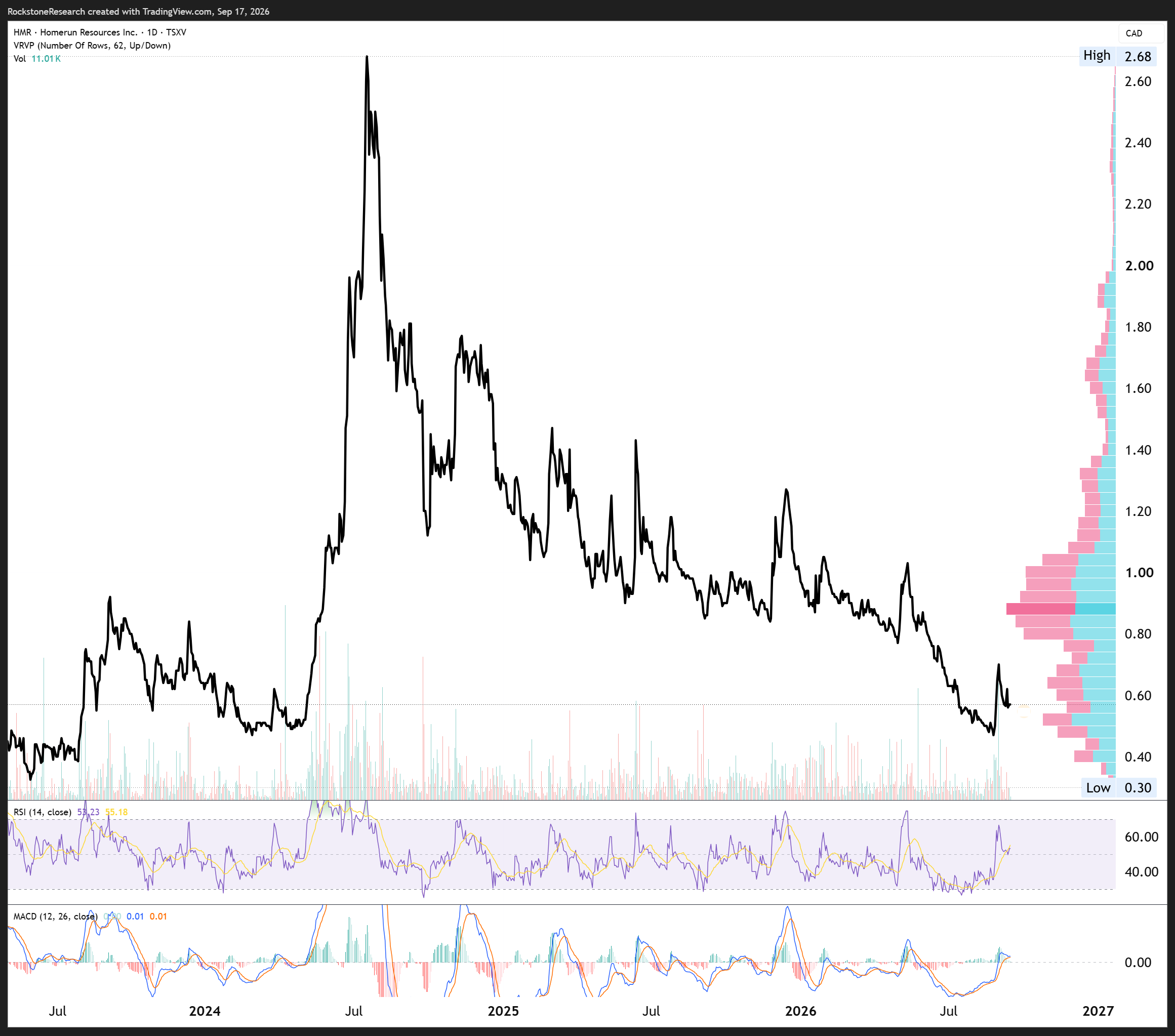
Canada Symbol (TSX.V): HMR
Current Price: 0.57 CAD (09/16/2026)
Market Capitalization: 44 Million CAD
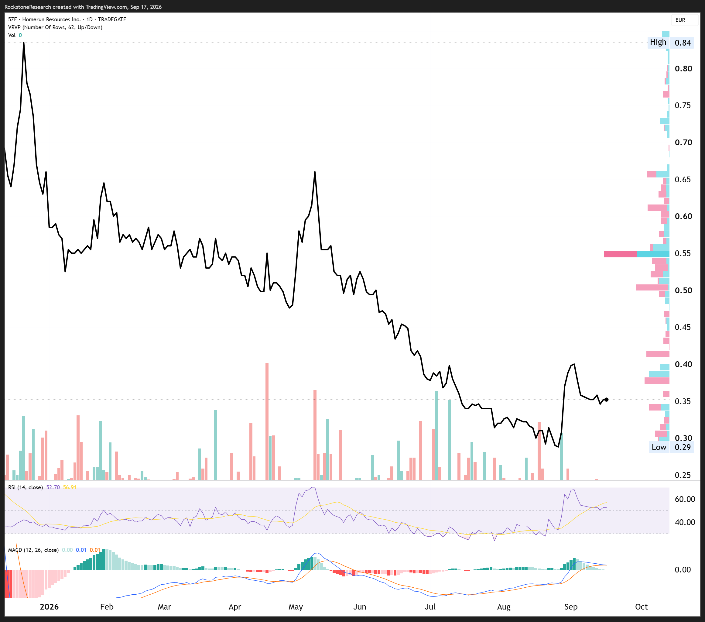
Germany Symbol / WKN: 5ZE / A3CYRW
Current Price: 0.352 EUR (09/16/2026)
Market Capitalization: 27 Million EUR

Stephan Bogner
Contact
Rockstone News & Research
Stephan Bogner (Dipl. Kfm., FH)
Müligässli 1, 8598 Bottighofen
Switzerland
Phone: +41-71-5896911
Email: info@rockstone-news.com
Disclaimer and Information on Forward Looking Statements: Rockstone and Homerun Resources Inc. (“Homerun“) caution investors that any forward-looking information provided herein is not a guarantee of future results or performance, and that actual results may differ materially from those in forward-looking information as a result of various factors. The reader is referred to Homerun’s public filings for a more complete discussion of such risk factors and their potential effects, which may be accessed through its documents filed on SEDAR+ at www.sedarplus.ca. All statements in this report, other than statements of historical fact, should be considered forward-looking statements. Much of this report is comprised of statements of projection, interpretation and strategic analysis. Such statements involve known and unknown risks, uncertainties and other factors that may cause actual results, developments or events to differ materially from those anticipated in these forward-looking statements. There can be no assurance that such statements will prove to be accurate, as actual results and future events could differ materially from those anticipated in such statements. Forward-looking statements in this report include statements, interpretations, conclusions, strategic observations and analytical opinions regarding Homerun Resources Inc.’s high-purity silica resources in Bahia, Brazil, the Company’s Memorandum of Understanding with CEITEC S.A., the potential development, production and qualification of silicon carbide (SiC) materials, substrates and wafers, and Homerun’s broader strategy of advancing its silica into higher-value semiconductor and advanced-material applications. Forward-looking statements include, without limitation, expectations regarding the ability of Homerun and CEITEC to develop specific technical work programs under the MOU; the ability to process Homerun’s silica into silicon, high-purity SiC materials, SiC crystals, substrates or wafers; the suitability of such materials for semiconductor applications; and the ability to achieve the purity, crystal quality, defect density, consistency, yields, performance and cost characteristics required by semiconductor manufacturers. Statements regarding the potential role of CEITEC in providing technical specifications, semiconductor manufacturing expertise, validation or other support, and statements regarding Homerun’s potential role in developing or coordinating raw-material processing and manufacturing steps associated with semiconductor-grade SiC substrates and wafers, are forward-looking. The MOU expressly contemplates the potential production of semiconductor-grade SiC substrates and wafers by Homerun for offtake by CEITEC; however, it does not constitute a definitive commercial offtake agreement or guarantee that qualified commercial products, purchase commitments or revenues will result. Statements regarding Homerun’s ability to move progressively further along the semiconductor value chain, retain greater economic value from its silica resources within Brazil, develop domestic processing capabilities or participate in Brazil’s expanding semiconductor industry are also forward-looking. Such outcomes will depend on successful technical development, access to specialized equipment and expertise, manufacturing partnerships, qualification, customer acceptance, financing and commercial execution. Statements regarding Brazil’s semiconductor policy, CEITEC’s modernization, government support for silicon carbide technologies and the potential development of a broader domestic semiconductor ecosystem are based on publicly available information and current government and industry initiatives. There can be no assurance that funding levels, industrial policies, strategic priorities, implementation schedules or government programs will continue as currently contemplated. Statements regarding future growth in silicon carbide power electronics, electric vehicles, charging infrastructure, renewable-energy systems, energy storage, industrial applications, AI data centers and other end markets are based on third-party industry forecasts and publicly available information. Such forecasts are inherently uncertain, and actual market growth, capacity utilization, pricing, technology adoption and competitive conditions may differ materially from current expectations. Technical development and scale-up risks: The development of semiconductor-grade SiC materials, substrates and wafers involves substantial technical complexity. The contemplated pathway may include silica purification, silicon production, SiC synthesis, crystal growth, boule preparation, wafer slicing, polishing, epitaxy and subsequent semiconductor manufacturing steps. There can be no assurance that Homerun, CEITEC or future technology partners will successfully develop, integrate or scale these processes or achieve commercially acceptable purity, crystal quality, yields, defect levels, consistency or production economics. Material quality and qualification risks: Semiconductor-grade SiC requires stringent material specifications. Crystal defects, impurities, wafer quality, surface preparation and process consistency can affect semiconductor performance, reliability and manufacturing yield. Homerun has not demonstrated commercial production of semiconductor-grade SiC substrates or wafers, and there can be no assurance that materials derived from its silica resources will ultimately satisfy the requirements of CEITEC or other semiconductor manufacturers across different device types and operating conditions. Commercial adoption would require further testing, validation and qualification. Qualification cycles in the semiconductor industry can be lengthy, and successful technical development does not necessarily result in customer acceptance or commercial orders. CEITEC cooperation risks: The cooperation with CEITEC is currently governed by a Memorandum of Understanding and remains at an early stage. Future activities may depend on subsequent technical programs, agreements, funding, access to facilities, availability of personnel and alignment between the parties. There can be no assurance that the cooperation will result in commercial production, supply agreements, joint ventures, revenue or other economic benefits to Homerun. CEITEC is a state-owned Brazilian company and its activities, funding and strategic priorities may be influenced by government policy, public-sector budgeting and broader political or industrial objectives. Silicon carbide market and competitive risks: The global SiC industry is technologically demanding, capital intensive and highly competitive. Established producers possess significant experience in crystal growth, substrate manufacturing, epitaxy, semiconductor fabrication and customer qualification. Homerun may face competition from vertically integrated semiconductor companies, established substrate manufacturers and other advanced-material suppliers with substantially greater technical, financial and manufacturing resources. Although long-term SiC demand is expected to grow, the industry has also experienced periods of capacity expansion, pricing pressure and lower utilization. Market growth does not guarantee attractive economics for individual producers. Commercial success will depend on cost competitiveness, product quality, yields, scale, differentiation and customer acceptance. Capital, partnership and execution risks: Advancing from high-purity silica toward semiconductor-grade SiC substrates and wafers may require substantial additional technical development, specialized equipment, capital investment and cooperation with third-party technology and manufacturing partners. Homerun may need to develop certain processing capabilities internally while accessing others through external specialists. There can be no assurance that suitable partners, technology, equipment or financing will be available on acceptable terms or that contemplated development programs will proceed according to current expectations, schedules or budgets. Brazilian industrial strategy and supply-chain risks: Statements regarding Homerun’s potential role in strengthening Brazil’s domestic semiconductor supply chain, increasing domestic value addition or reducing dependence on imported semiconductor technologies represent strategic interpretations based on current public initiatives. There can be no assurance that Brazilian industrial policy, incentives, funding programs or procurement priorities will evolve in a manner favorable to Homerun. The development of a more complete domestic SiC value chain would require capabilities extending beyond raw materials, including crystal growth, wafer processing, epitaxy, device manufacturing, packaging, testing and qualification. Some of these capabilities may need to be developed or accessed through third parties. Commercialization risks: There can be no assurance that Homerun will successfully produce commercial semiconductor-grade SiC materials, substrates or wafers, establish customer relationships, achieve competitive production costs or generate revenue from the applications discussed in this report. Technical feasibility, commercial viability and market acceptance remain to be demonstrated. Potential economic value associated with advancing Homerun’s silica further along the semiconductor value chain is therefore speculative at this stage and will depend on successful execution of multiple technical and commercial milestones. Forward-looking analytical opinions: This report contains the author’s independent analysis and interpretation of publicly available information. Statements regarding the strategic significance of the CEITEC cooperation, the potential importance of CEITEC’s semiconductor infrastructure, the relevance of Brazil’s SiC investments, Homerun’s ability to advance its silica toward higher-value semiconductor materials, the potential benefits of greater domestic value addition and the economic significance of moving further along the semiconductor value chain represent analytical opinions rather than statements of fact. Statements suggesting that Homerun’s silica resource could serve as the starting point for a broader advanced-materials strategy or that the Company could ultimately participate in SiC substrate, wafer or semiconductor supply chains are forward-looking and subject to the technical, financial, commercial and execution risks described above. Such opinions are inherently subjective and should not be interpreted as guarantees of technical success, commercial-scale production, customer qualification, commercial agreements, market adoption, competitive advantage, financing, profitability, shareholder value creation or future market performance. Accordingly, readers should not place undue reliance on forward-looking information. Actual results may differ materially from those expressed or implied in the forward-looking statements contained in this report. Rockstone and the author of this report do not undertake any obligation to update any statements made herein except as required by applicable law. Past performance, comparisons to other companies, projects, commodities, technologies, jurisdictions, feasibility studies, capital-market events or industry trends are provided for illustrative purposes only and should not be considered indicative of future results.
Disclosure of Interest and Advisory Cautions: Nothing in this report should be construed as a solicitation to buy or sell any securities mentioned. Rockstone, its owners and the author of this report are not registered broker-dealers or financial advisors. Before investing in any securities, you should consult with your financial advisor and a registered broker-dealer. Never make an investment based solely on what you read in an online or printed report, including Rockstone’s report, especially if the investment involves a small, thinly-traded company that isn’t well known. The author of this report, Stephan Bogner, is paid by Homerun Resources Inc. On September 8, 2025, Homerun announced that the company “entered into an agreement with Rockstone Research to provide marketing services to the company”, and that “Rockstone Research is an arm’s-length marketing firm and has been engaged for an initial three-month term for total consideration of $25,000, which is payable up front. The company does not propose to issue any securities to Rockstone in consideration for the services to be provided to the company.” The marketing services agreement has since been extended and remains in effect as of the date of this report. The author owns equity of Homerun and thus will profit from volume and price appreciation of the stock. This also represents a significant conflict of interest that may affect the objectivity of this reporting. The author may buy or sell securities of Homerun (or comparable companies) at any time without notice, which may give rise to additional conflicts of interest. Overall, multiple conflicts of interests exist. Therefore, the information provided in this report should not be construed as a financial analysis or recommendation but as an advertisement. This report should be understood as a promotional publication and does not replace individual investment advice. Rockstone’s and the author’s views and opinions regarding the companies that are featured in the reports are the author‘s own views and are based on information that was received or found in the public domain, which is assumed to be reliable. Rockstone and the author have not undertaken independent due diligence of the information received or found in the public domain. Rockstone and the author of this report do not guarantee the accuracy, completeness, or usefulness of any content of this report, nor its fitness for any particular purpose. Lastly, Rockstone and the author do not guarantee that any of the companies mentioned in the reports will perform as expected, and any comparisons that were made to other companies may not be valid or come into effect. For the avoidance of doubt, this report is not intended for distribution to, or use by, any person or entity in any jurisdiction where such distribution, publication or use would be contrary to local law or regulation. Readers are solely responsible for ensuring that their review and use of this report is lawful in their jurisdiction. Neither Rockstone nor the author accepts liability for any direct or indirect loss arising from the use of this report or from any investment decision made in reliance on it. Please read the entire Disclaimer carefully. If you do not agree to all of the Disclaimer, do not access this website or any of its pages including this report in form of a PDF. By using this website and/or report, and whether or not you actually read the Disclaimer, you are deemed to have accepted it. Information provided is educational and general in nature and should not be interpreted as personalized investment, financial, legal, tax or professional advice. Data, tables, figures and pictures, if not labeled or hyperlinked otherwise, have been obtained from Stockwatch.com, Tradingview.com, Homerun Resources Inc. and the public domain.


