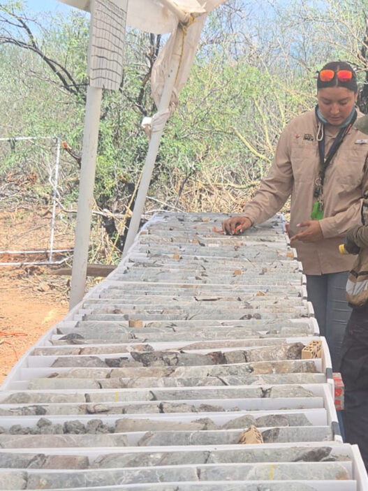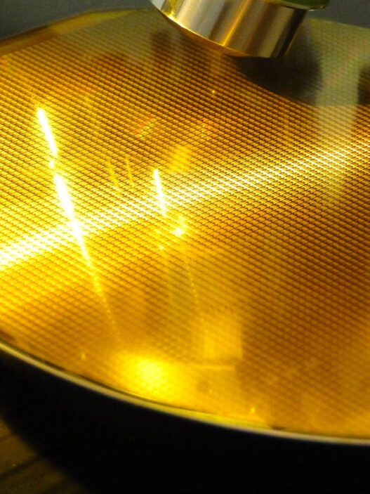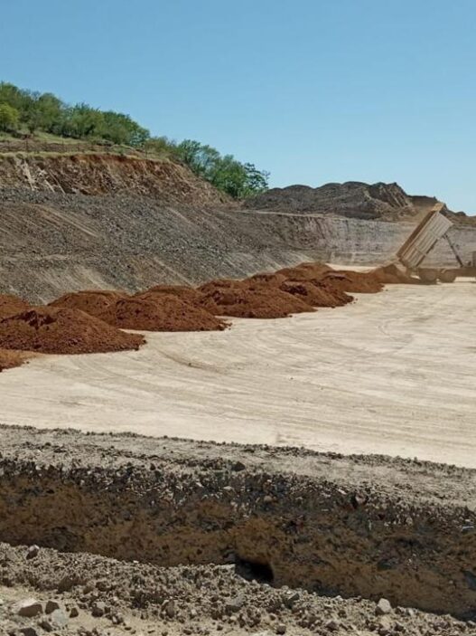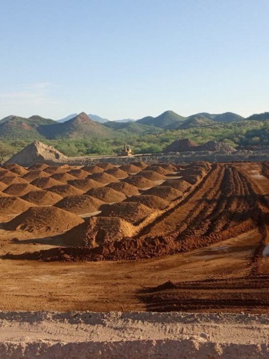


It begins with sand. At Santa Maria Eterna in Bahia, Brazil, Homerun Resources Inc.controls an unusually pure silica resource that has already become the foundation of its planned solar-glass business. Now that same material is being pushed toward an entirely different technological frontier.
In today’s news-release, Homerun describes work with the University of California, Davis to process SME silica into fused silica, silicon and silicon carbide suitable for semiconductor feedstocks and substrates. UC Davis has also developed a patent-pending laser purification process using Homerun’s material that has achieved purity above 4N, or 99.99% SiO₂, without chemical purification inputs.
Behind the chemistry and processing terminology in today’s news lies a much larger strategic idea: How far can an exceptional raw material travel up the value chain? For Homerun, the answer extends far beyond solar glass.
What begins as a grain of unusually pure silica in Bahia is now being pushed toward a very different frontier: Fused silica, silicon, silicon carbide, semiconductors, photonics and, eventually, quantum technologies.
Each step moves the material further away from conventional industrial-minerals markets and deeper into some of the most advanced technology value chains in the world.
That is what makes today’s announcement so important: Homerun is not simply adding another possible end market. It is beginning to show how a single high-purity resource could become the foundation for multiple downstream industries, each with higher technical barriers, higher material requirements and potentially far greater value.
The journey starts in sand. The destination is technology. And the gap between them is beginning to close.
TURNING PURITY INTO TECHNOLOGY
The pathway now being developed runs from high-purity silica through purification and advanced processing into silicon and silicon carbide, with potential applications further downstream in semiconductors, integrated photonics and eventually quantum technologies.
As the material moves deeper into these industries, purity becomes increasingly critical. Advanced semiconductor and photonics applications demand extraordinary consistency and extremely low concentrations of unwanted elements. The quality of the starting material therefore matters long before a wafer is produced or a photonic circuit begins transmitting light.
This is where Homerun’s potential competitive advantage begins: An unusually clean natural feedstock that can serve as the foundation for progressively higher-value processing steps. Solar glass represents one expression of that strategy. Silicon and silicon carbide could become another, opening the door to far more advanced technology markets.
THE RISE OF SILICON CARBIDE
Silicon carbide is already an important material in electric vehicles, power electronics and high-voltage infrastructure. Its relevance is expanding further as artificial intelligence (AI) transforms data-center architecture.
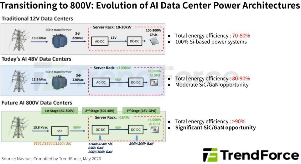
AI systems require enormous computing power, but moving the resulting quantities of data between processors is becoming a major technological and energy bottleneck. That is driving the industry toward optical communication, where information travels using light.
The numbers illustrate how quickly this transition is accelerating: TrendForce expects the global market for AI-focused optical transceivers to increase from approximately 16.5 billion USD in 2025 to 26 billion USD in 2026, representing growth of more than 57% in a single year. Modules operating at 800G and above are expected to represent more than 60% of global optical-transceiver shipments by 2026.
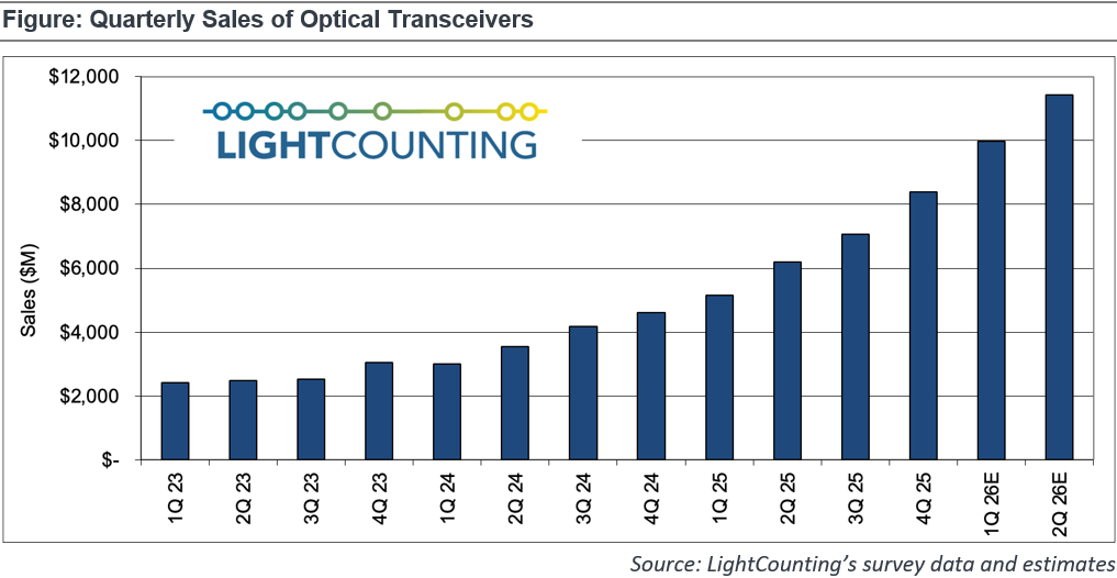
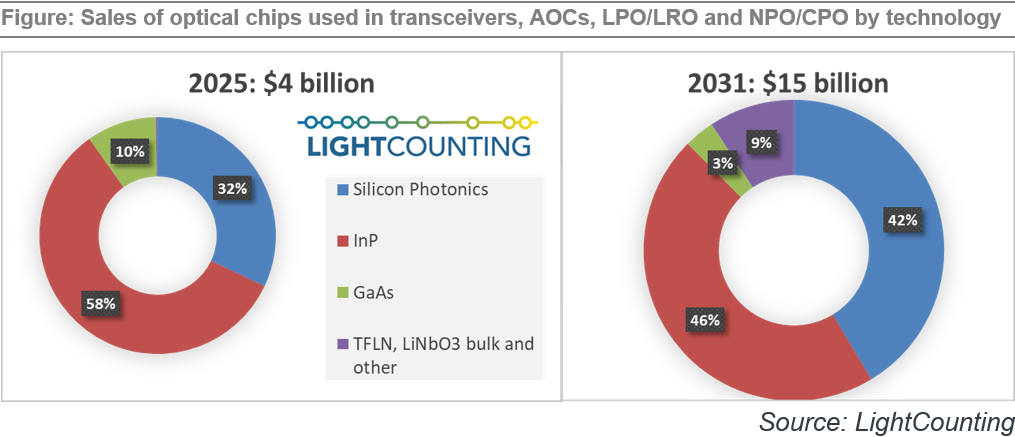
Silicon photonics is moving alongside that expansion: LightCounting expects sales of silicon-photonics chips to grow by ~110% in 2026. It also estimates that 2026 will be the first year in which optical transceivers using silicon-photonics modulators account for more than half of the roughly 40 billion USD global transceiver market.
And commercial deployment is already beginning: In July, TrendForce reported that NVIDIA had begun shipping its next-generation Spectrum-X co-packaged-optics switch to selected partners, while Broadcom’s 51.2T Bailly CPO switch had entered volume manufacturing. TrendForce described these developments as marking the official transition of co-packaged optics into the mass-production phase. Around the same time, UMC announced the first delivery of mass-produced 12-inch silicon-photonics wafers from its Singapore fab, supporting next-generation 1.6T connectivity for AI and hyperscale data centers.
The shift toward photonics is therefore becoming an industrial reality.
AI IS UNLEASHING A NEW INVESTMENT SUPERCYCLE
The wider backdrop is equally striking: Global semiconductor sales reached 403.3 billion USD in the second quarter of 2026 alone, according to the Semiconductor Industry Association (SIA), representing a 35.1% increase over the first quarter. June sales reached 134.5 billion USD, and the SIA currently expects global semiconductor sales to exceed 1.5 trillion USD in 2026.
Much of the infrastructure investment behind this growth is tied directly to AI: TrendForce estimates that the world’s 9 largest cloud service providers (Google, Amazon, Meta, Microsoft, Oracle, ByteDance, Tencent, Alibaba and Baidu) will spend more than 886.7 billion USD in capital expenditures during 2026, ~90% more than a year earlier. AI-server shipments are meanwhile forecast to rise by almost 31%.
This investment is no longer confined to GPUs. It is spreading into power systems, cooling, advanced packaging and increasingly the high-speed optical infrastructure connecting enormous AI clusters. That creates a powerful industrial backdrop for advanced silicon materials.
Silicon carbide (SiC) itself is also increasingly entering AI infrastructure through power electronics: TrendForce notes that SiC and GaN are moving into large-scale deployment as data centers confront what it calls the AI “power wall”, with high-voltage architectures requiring more efficient semiconductor materials.
Homerun’s exploration of silicon carbide therefore touches 2 major technological shifts simultaneously: The power infrastructure behind AI and the photonic infrastructure connecting AI computing systems.
BRAZIL MEETS CALIFORNIA
That brings the story back to Bahia. The raw material comes from Brazil. The advanced materials research is being carried out with UC Davis in California. The targeted markets sit within some of the most sophisticated technology supply chains in the world.
This creates a potentially important bridge between Brazilian geology and North American materials science, linking a naturally advantaged feedstock with the research capabilities needed to move it into far more demanding technology applications.
At a time when governments and corporations are placing increasing emphasis on diversified, secure supply chains less dependent on China, Homerun’s geographic positioning could become strategically relevant.
The SME “Silica Valley” is therefore beginning to look like more than the geological foundation of a solar-glass project. It is increasingly becoming the common starting point for several different industrial pathways.
UNLOCKING MULTIPLE VALUE CHAINS
Solar glass remains the most advanced. Homerun’s planned solar glass project in Bahia is the clearest industrial expression of the company’s vertical-integration strategy today.
However, behind that project, another picture is emerging: The same silica resource is now being connected with energy storage, advanced silica materials, silicon, silicon carbide and photonics.
Each vertical sits at a different stage of development. What connects them is the SME silica itself. That common starting point creates the possibility of building several downstream businesses around a single resource base, while allowing advances in purification, processing and materials science to support more than a single end market. That is ultimately what makes the story unusual.
A single geological asset may have the potential to feed multiple value chains whose end markets look almost unrelated to one another: Glass, energy storage, semiconductors, photonics and quantum technologies. Yet they all begin with the same grain of sand.
THE MEANING BEHIND THE TECHNICAL DEPTH
That helps explain the unusual character of Homerun’s latest announcement. The news-release goes deep into purification, precursor production, rapid thermal processing, single-crystal growth, wafer preparation, photonic devices and quantum-network architectures.
For many investors, the level of detail may appear excessive. For industrial and technology counterparties, those details are where the real questions begin.
Purity, scalability, energy intensity, repeatability and material specifications all matter. Whether a feedstock can move successfully from laboratory work into an industrial process depends on these parameters.
Seen in that light, today’s news reads almost like a technical map of where Homerun wants its silica to travel.
CEO Brian Leeners also notes that the company’s efforts are attracting “strategic global attention” across the materials sectors it is targeting. That may prove to be one of the more important lines in the entire announcement.
IT ALL BEGINS WITH SILICA
The larger Homerun story is starting to change. For a long time, Homerun could largely be summed up in 3 words: Silica and solar glass. That description is becoming too narrow.
The SME “Silica Valley” may ultimately support a much broader materials platform, with solar glass representing the most advanced industrial development and silicon, silicon carbide and photonics opening an earlier-stage pathway toward some of the highest-value technology markets in existence.
The underlying philosophy remains remarkably simple: Begin with an unusually pure raw material and keep moving it toward higher-value applications.
The timing is striking:
- Global semiconductor sales are surging.
- AI infrastructure spending is approaching unprecedented levels.
- Optical-transceiver markets are expanding rapidly.
- Silicon photonics is entering mass production.
- Co-packaged optics is beginning its commercial ramp.
- Silicon carbide is becoming increasingly important to AI power infrastructure, while advanced photonics is transforming the communications infrastructure connecting AI systems.
And beneath all of those technologies, before the chips, the data centers, the photonic networks and the quantum devices, lies something far more basic: The raw materials that make them possible.
Homerun’s SME “Silica Valley” sits at one of those starting points. A grain of sand in Bahia may appear a very long way from an AI data center, a photonic chip or a quantum network. Technologically, it is. Yet every one of those systems begins with materials – and strategically, that distance is beginning to shrink.
The question is no longer merely how much silica Homerun controls. The question is what that silica can ultimately become.
BOTTOM LINE
Homerun’s latest technical update adds another layer to a story that is becoming much broader than solar glass.
The significance lies in the fact that the company is working to connect a naturally high-purity silica resource in Bahia with some of the fastest-growing technology value chains in the world. The pathway now being developed with UC Davis reaches from silica purification into fused silica, silicon and silicon carbide, with potential applications in semiconductors, integrated photonics and eventually quantum technologies.
At the same time, the external market backdrop surrounding these technologies is accelerating rapidly. AI infrastructure investment is driving massive demand for power efficiency, high-speed optical connectivity and new semiconductor architectures.
Silicon carbide is gaining importance in high-voltage power systems, while silicon photonics and co-packaged optics are moving into commercial production. The charts included in this report illustrate just how quickly these markets are scaling.
For Homerun, the strategic opportunity sits at the very beginning of these value chains. The company does not need to become a chip manufacturer to participate in their growth. Its opportunity is to establish SME silica as a secure, high-purity feedstock that can move through increasingly sophisticated processing stages and into markets where purity, consistency and material performance matter enormously, creating exposure to several advanced industries from a single resource base.
Solar glass remains the most advanced industrial expression of this strategy today. But the emerging silicon, silicon-carbide and photonics pathway demonstrates how much broader the underlying platform could become.
The bigger picture is simple: Homerun is building value around a single exceptional raw material by moving it into progressively higher-value applications.
As that strategy advances, the significance of the SME “Silica Valley” may ultimately be measured not only by how much silica it contains, but by how many high-value technology chains can be built upon it.
Company Details

Homerun Resources Inc.
#2110 – 650 West Georgia Street
Vancouver, BC, V6B 4N7 Canada
Phone: +1 844 727 5631
Email: info@homerunresources.com
www.homerunresources.com
ISIN: CA43758P1080 / CUSIP: 43758P
Shares Issued & Outstanding: 77,333,285
Canada Symbol (TSX.V): HMR
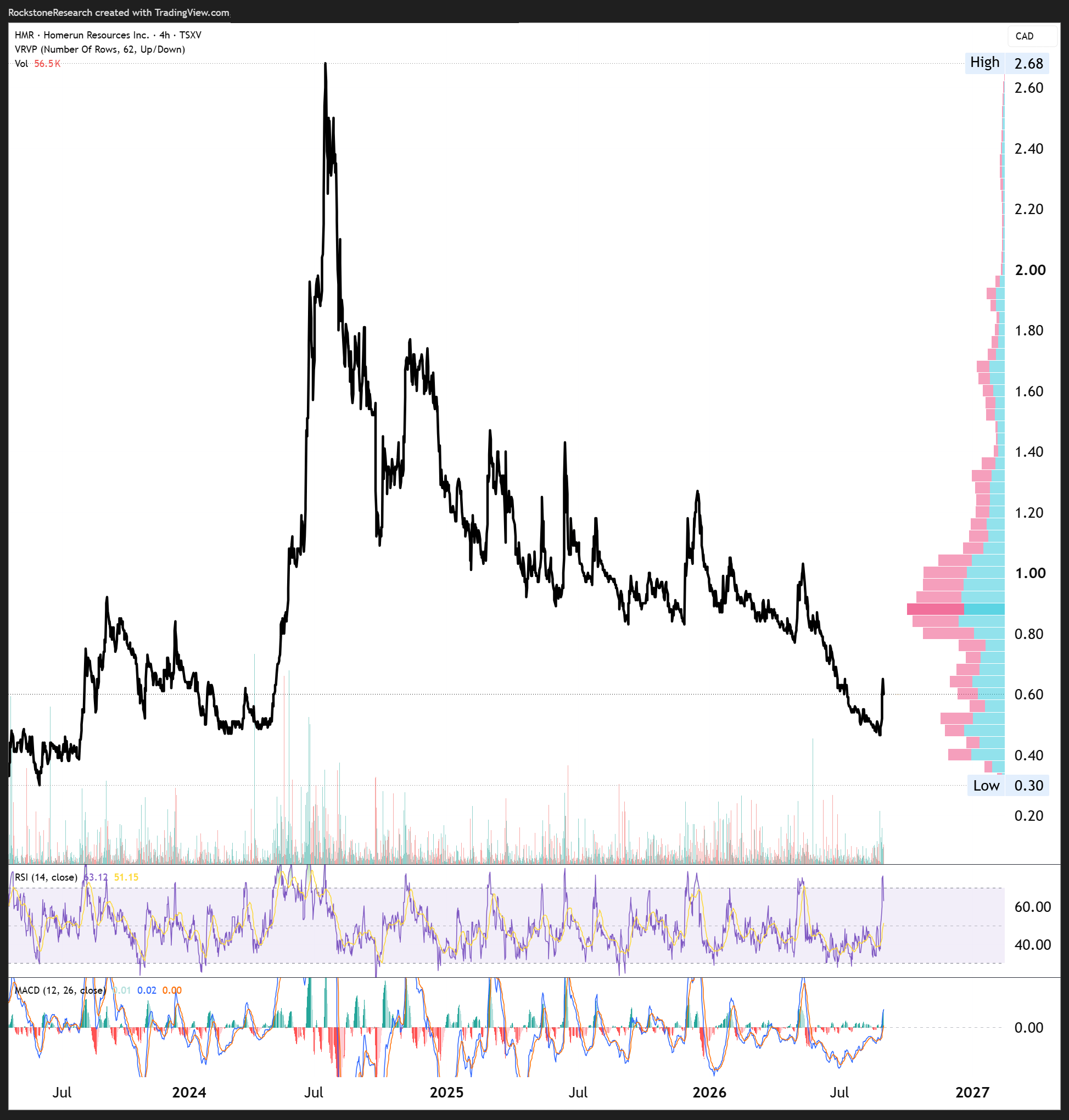
Current Price: 0.57 CAD (08/31/2026)
Market Capitalization: 44 Million CAD
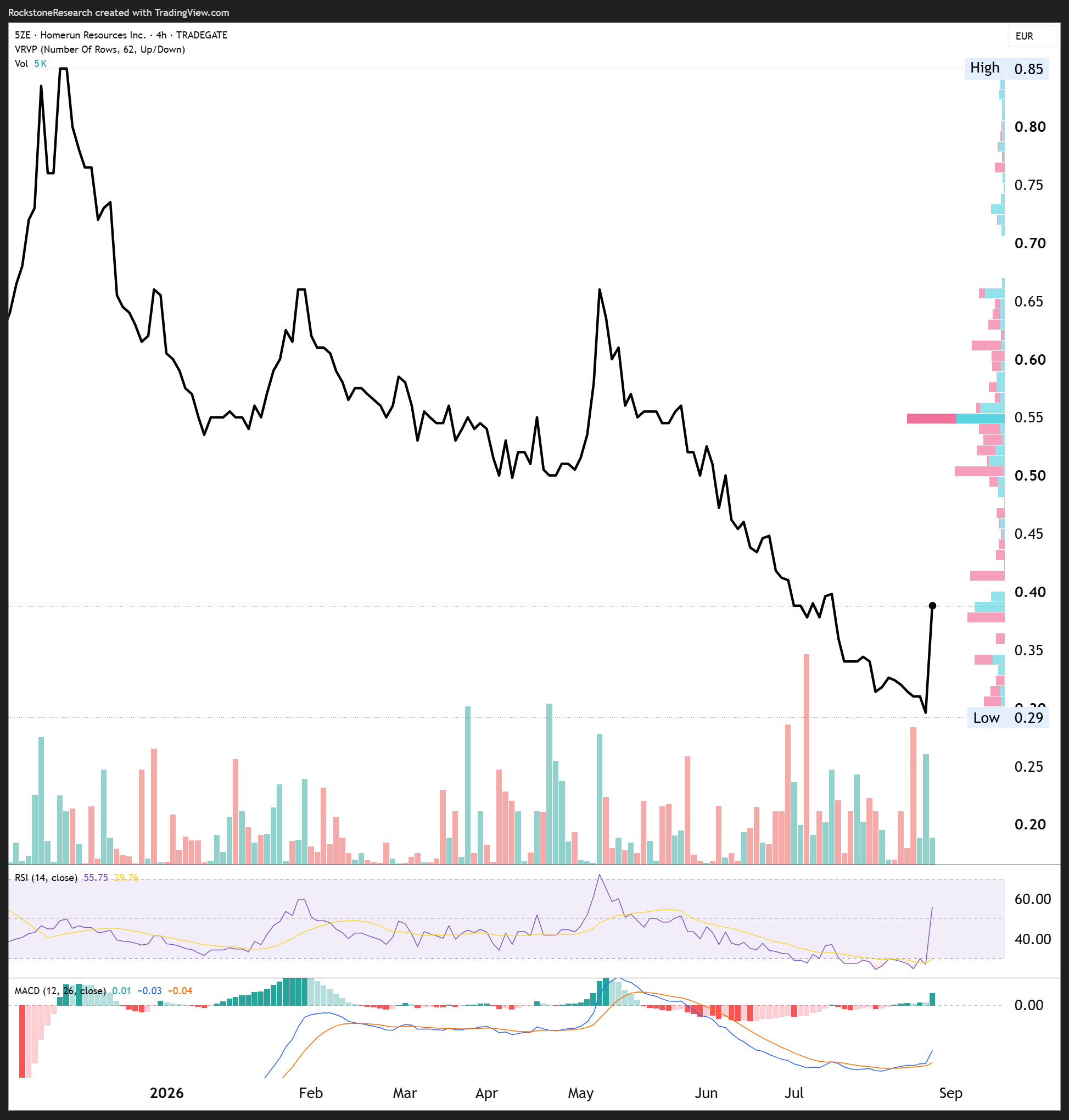
Germany Ticker / WKN: 5ZE / A3CYRW
Current Price: 0.358 EUR (08/31/2026)
Market Capitalization: 28 Million EUR

Stephan Bogner
Contact
Rockstone News & Research
Stephan Bogner (Dipl. Kfm., FH)
Müligässli 1, 8598 Bottighofen
Switzerland
Phone: +41-71-5896911
Email: info@rockstone-news.com
Disclaimer and Information on Forward Looking Statements: Rockstone and Homerun Resources Inc. (“Homerun“) caution investors that any forward-looking information provided herein is not a guarantee of future results or performance, and that actual results may differ materially from those in forward-looking information as a result of various factors. The reader is referred to Homerun’s public filings for a more complete discussion of such risk factors and their potential effects, which may be accessed through its documents filed on SEDAR+ at www.sedarplus.ca. All statements in this report, other than statements of historical fact, should be considered forward-looking statements. Much of this report is comprised of statements of projection, interpretation and strategic analysis. Such statements involve known and unknown risks, uncertainties and other factors that may cause actual results, developments or events to differ materially from those anticipated in these forward-looking statements. There can be no assurance that such statements will prove to be accurate, as actual results and future events could differ materially from those anticipated in such statements. Forward-looking statements in this report include statements, interpretations, conclusions, strategic observations and analytical opinions regarding Homerun’s high-purity silica resources in the Santa Maria Eterna (SME) Silica Valley in Bahia, Brazil, the Company’s collaboration with the University of California, Davis (UC Davis), the development and potential commercialization of purification and processing technologies, the patent-pending laser purification process, the production of fused silica, silicon and silicon carbide (SiC), potential semiconductor and photonics applications, Silicon Carbide-on-Insulator (SiCOI) platforms, integrated photonics, quantum technologies, AI infrastructure, energy-storage applications, solar glass and Homerun’s broader vertically integrated silica strategy. Forward-looking statements include, without limitation, expectations regarding the ability of Homerun and its research collaborators to further develop, optimize, scale and commercialize processes for upgrading SME silica into increasingly high-purity and higher-value materials; the suitability of SME silica for downstream applications; the ability to achieve required purity, consistency, impurity control, material performance, production yields and cost parameters; and the potential for Homerun’s silica to become a feedstock for advanced semiconductor, silicon carbide, photonics and other technology value chains. Forward-looking statements also include expectations regarding the significance and scalability of the patent-pending laser purification process developed through the UC Davis collaboration, including its potential ability to achieve high-purity silica without chemical purification inputs, reduce processing complexity or environmental impacts, and contribute to commercially viable purification pathways. Laboratory or research results, including reported purity levels above 4N, may not necessarily be reproducible at commercial scale or sufficient for all contemplated semiconductor, photonic or quantum applications. Statements regarding the potential conversion of SME silica into fused silica, silicon and silicon carbide and the use of such materials in semiconductor feedstocks, substrates, wafers, power electronics, integrated photonics, AI infrastructure and quantum technologies are forward-looking. The development of these applications remains subject to further technical development, testing, qualification, engineering, scale-up, customer acceptance, commercial agreements and capital availability. Statements regarding future growth in semiconductor markets, artificial-intelligence infrastructure spending, optical-transceiver demand, silicon-photonics adoption, co-packaged optics, silicon-carbide deployment and quantum technologies are based on third-party industry forecasts and publicly available information. Such forecasts are inherently uncertain and actual market growth, adoption rates, capital expenditures, technological pathways and commercial outcomes may differ materially from current estimates. Statements regarding the Company’s ability to establish secure, diversified or non-China supply chains, develop commercial relationships with technology companies, semiconductor manufacturers, materials processors or other industrial counterparties, and position its Brazilian silica resources within North American or global advanced-materials supply chains are also forward-looking. Such statements are based on current management expectations, publicly available information and the author’s independent analysis and remain subject to numerous risks, uncertainties and assumptions. Technical Development and Scale-Up Risks: Research-stage and laboratory-scale results may not translate into commercially viable processes. The contemplated value chain, including purification, precursor synthesis, thermal processing, silicon and silicon carbide production, crystal growth and wafer fabrication, involves substantial technical complexity. There can be no assurance that Homerun or its collaborators will successfully reproduce laboratory results at pilot or commercial scale, achieve required product specifications, obtain acceptable yields, maintain consistent impurity control or develop processes that are economically competitive with established technologies. Purity and Product Qualification Risks: Advanced semiconductor, photonics and quantum applications can require extremely stringent purity, defect-density and material-performance specifications. Different applications may require substantially different purity levels and impurity profiles. Reported purity levels achieved during research and development, including +4N purity, should not be interpreted as confirmation that Homerun’s materials presently satisfy semiconductor-grade, photonics-grade or quantum-grade specifications for any particular commercial application. Commercial adoption would require further testing, validation and qualification by prospective customers and industry participants. Intellectual Property and Technology Risks: The laser purification technology described in this report is patent-pending. There can be no assurance that any patent application will result in issued patents, that issued patents will provide meaningful commercial protection, or that competing technologies will not emerge. Homerun’s future ability to benefit commercially from purification, processing or advanced-material technologies may depend upon intellectual-property rights, licensing arrangements, research agreements, proprietary know-how and continued access to technical expertise. Semiconductor, Silicon Carbide and Photonics Commercialization Risks: The semiconductor, silicon-carbide and photonics industries are technologically demanding, capital intensive and highly competitive. Commercial participation may require significant additional investment, specialized equipment, manufacturing partnerships, customer qualification processes, reliable high-volume production and compliance with stringent industry standards. There can be no assurance that Homerun will successfully enter these markets, establish commercial supply relationships, achieve competitive production costs or capture meaningful market share. AI Infrastructure and Market Adoption Risks: Statements regarding the growth of AI data centers, optical interconnects, silicon photonics, co-packaged optics and silicon-carbide power electronics are based in part on current market trends and third-party forecasts. The pace and direction of technology adoption may change due to economic conditions, customer preferences, competing architectures, technological breakthroughs, supply-chain developments, regulatory changes or capital-spending reductions. Growth in the underlying markets does not necessarily translate into demand for Homerun’s products or commercial success for the Company. Supply-Chain and Strategic Positioning Risks: Statements regarding the strategic importance of diversified, secure or non-China supply chains represent management expectations and analytical interpretations. There can be no assurance that geopolitical developments, government policies, trade measures, industrial incentives or customer procurement strategies will develop in a manner favorable to Homerun or that the Company will become a material supplier to semiconductor, photonics, silicon-carbide or other advanced-technology supply chains. Financing, Construction and Execution Risks: Homerun’s broader strategy, including its Solar Glass Project and development of advanced silica-material pathways, may require substantial additional financing, engineering, procurement, infrastructure, equipment, permitting, construction and technical resources. Capital costs, operating costs, energy requirements, equipment availability, contractor performance, labour availability, foreign exchange movements, inflation, supply-chain conditions and project schedules may differ materially from current assumptions. There can be no assurance that sufficient financing will be secured or that contemplated projects will proceed on schedule, within budget or in accordance with current plans. Commercial and Market Risks: Statements regarding future demand for solar glass, high-purity silica, fused silica, silicon, silicon carbide, semiconductor materials, photonics and related applications are forward-looking. Commercial success will depend upon product qualification, customer acceptance, competitive pricing, production reliability, market growth, technological developments, substitution risks, competing materials and processes, international trade policies and broader economic conditions. Strategic and Multi-Vertical Development Risks: Homerun is pursuing several downstream opportunities from a common high-purity silica resource, including solar glass, energy storage, advanced silica materials, silicon, silicon carbide and photonics. These verticals are at different stages of technical and commercial development and may require different technologies, partners, capital requirements and commercialization pathways. There can be no assurance that all contemplated verticals will be successfully developed or that technical advances in one area will translate into commercial advantages in another. Forward-Looking Analytical Opinions: This report contains the author’s independent analysis and interpretation of publicly available information. Statements regarding the strategic significance of Homerun’s UC Davis collaboration, the importance of the patent-pending laser purification process, the potential competitive advantage of SME silica, the Company’s ability to move progressively further downstream, the potential relevance of Homerun’s silica to semiconductor, silicon-carbide, photonics, AI-infrastructure or quantum-technology value chains, and the evolution of Homerun from a silica and solar-glass company toward a broader advanced-materials platform represent analytical opinions rather than statements of fact. Such opinions are inherently subjective and should not be interpreted as guarantees of technical success, commercial-scale production, customer qualification, commercial agreements, market adoption, competitive advantage, financing, profitability, shareholder value creation or future market performance. Accordingly, readers should not place undue reliance on forward-looking information. Actual results may differ materially from those expressed or implied in the forward-looking statements contained in this report. Rockstone and the author of this report do not undertake any obligation to update any statements made herein except as required by applicable law. Past performance, comparisons to other companies, projects, commodities, technologies, jurisdictions, feasibility studies, capital-market events or industry trends are provided for illustrative purposes only and should not be considered indicative of future results.
Disclosure of Interest and Advisory Cautions: Nothing in this report should be construed as a solicitation to buy or sell any securities mentioned. Rockstone, its owners and the author of this report are not registered broker-dealers or financial advisors. Before investing in any securities, you should consult with your financial advisor and a registered broker-dealer. Never make an investment based solely on what you read in an online or printed report, including Rockstone’s report, especially if the investment involves a small, thinly-traded company that isn’t well known. The author of this report, Stephan Bogner, is paid by Homerun Resources Inc. On September 8, 2025, Homerun announced that the company “entered into an agreement with Rockstone Research to provide marketing services to the company”, and that “Rockstone Research is an arm’s-length marketing firm and has been engaged for an initial three-month term for total consideration of $25,000, which is payable up front. The company does not propose to issue any securities to Rockstone in consideration for the services to be provided to the company.” The marketing services agreement has since been extended and remains in effect as of the date of this report. The author owns equity of Homerun and thus will profit from volume and price appreciation of the stock. This also represents a significant conflict of interest that may affect the objectivity of this reporting. The author may buy or sell securities of Homerun (or comparable companies) at any time without notice, which may give rise to additional conflicts of interest. Overall, multiple conflicts of interests exist. Therefore, the information provided in this report should not be construed as a financial analysis or recommendation but as an advertisement. This report should be understood as a promotional publication and does not replace individual investment advice. Rockstone’s and the author’s views and opinions regarding the companies that are featured in the reports are the author‘s own views and are based on information that was received or found in the public domain, which is assumed to be reliable. Rockstone and the author have not undertaken independent due diligence of the information received or found in the public domain. Rockstone and the author of this report do not guarantee the accuracy, completeness, or usefulness of any content of this report, nor its fitness for any particular purpose. Lastly, Rockstone and the author do not guarantee that any of the companies mentioned in the reports will perform as expected, and any comparisons that were made to other companies may not be valid or come into effect. For the avoidance of doubt, this report is not intended for distribution to, or use by, any person or entity in any jurisdiction where such distribution, publication or use would be contrary to local law or regulation. Readers are solely responsible for ensuring that their review and use of this report is lawful in their jurisdiction. Neither Rockstone nor the author accepts liability for any direct or indirect loss arising from the use of this report or from any investment decision made in reliance on it. Please read the entire Disclaimer carefully. If you do not agree to all of the Disclaimer, do not access this website or any of its pages including this report in form of a PDF. By using this website and/or report, and whether or not you actually read the Disclaimer, you are deemed to have accepted it. Information provided is educational and general in nature and should not be interpreted as personalized investment, financial, legal, tax or professional advice. Data, tables, figures and pictures, if not labeled or hyperlinked otherwise, have been obtained from Stockwatch.com, Tradingview.com, Homerun Resources Inc. and the public domain. The cover picture has been obtained and licenced from 123rf.com.